收獲
????一晃五年~
????五年前那個夏夜,我對著泛藍的屏幕敲下《給十年后的自己》,在2020年的疫情迷霧中編織著對未來的想象。此刻回望,第四屆集創賽的參賽編號仍清晰如昨,而那個在家熬夜焊電路板的"不眠者",現在也漸漸熬不動夜了😹😹
????如果遇見五年前的自己,我想告訴他:當年在博客里追問的"職業門路",答案就藏在每個調試通宵的星光里;那些擔心被時代拋下的焦慮,終會熔鑄成攀登技術棧的勇氣。🙆🙆
????十年之約才過半程,職業的時鐘域仍在擴展,就像我們永遠年輕的技術信仰。下一個五年,愿芯片上的每一個邏輯門都通往星辰,愿每個深夜的堅持都能被未來溫柔解碼——因為代碼從不辜負時光,正如奮斗永遠眷顧追夢人。🍃 🍃

目錄
- 收獲
- 正文
- 1、參考文獻
- 2、Bitslip in Logic
- 2.1、現狀
- 2.2、bitslip原理
- 2.3、解決方案A
- 2.4、解決方案B
- 2.4.1、8B verilog代碼:
- 2.4.2、分析一下代碼
- 3、RX_BITSLICE功能
- 4、工程獲取
- 4.1、部分代碼
- 4.2、完整工程(含仿真)
- 總結
正文
1、參考文獻
本文主要講UltraScale+ bitslip方案,iserdese3等概念,有文章說過了,這里就不做贅述:
1、Ultrascale selectio 仿真之 ISERDESE3和OSERDESE3
2、ISERDESE3/OSERDESE3例化和仿真
3、LVDS系列11:Xilinx Ultrascale系可編程輸入延遲(一)
4、Xilinx IDELAYE3原語詳細解讀
5、iodelay 使用總結
(5這篇參數比較詳細)
本文工程會放在最后一節。
注意:
一些爭議點:
ISERDESE3有個地方,xilinx手冊可能有點歧義:
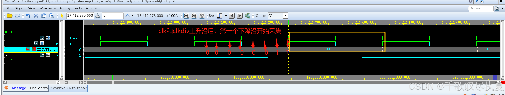
從手冊看,Q[7:0]的輸出是占了2個CLKDIV時鐘周期,但是實際仿真,只占了1個。
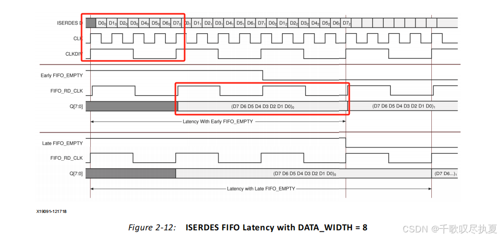
??????不管是其他博主的仿真,還是我自己仿的,都是1個clkdiv周期,有知道的朋友,可以評論區留言交流。
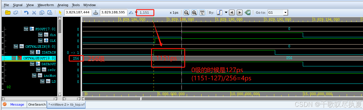
????看了幾篇文章,每篇文章一個tap多少ps說的總是有些出入,這里結合我的仿真,算了一下,一個tap是4ps(事實上,我在一個器件文檔里面是有提到硬件決定了這就是4ps的,但是忘記哪個文檔了):
????0級的時候,輸入和輸出直接的延遲是127ps;后面每次算,都要減去或者加上這個127ps。
有其他看法的朋友,也可以評論區交流。
2、Bitslip in Logic
2.1、現狀
??????這小節結論:ISERDESE3沒有bitslip功能了,需要用邏輯實現。(可以結合小結3的RX_BITSLICE結構圖看一下)
??????UltraScale器件中的I/O邏輯是指位于專用的I/O處理組件在I/O緩沖區和一般互連之間。這個I/O邏輯在UltraScale中是不同的。與以前的系列(如7系列和Virtex-6 fpga)相比,UltraScale器件中的I/O邏輯設置提供更快的I/O處理,更好的抖動規格,還有更多的功能。但是,它忽略了以前器件系列的I/O邏輯中可用的一些功能。
??????位滑(bitslip)是一個在UltraScale器件I/O邏輯中原生不可用的功能。這個應用程序注描述了在一般互連中實現的位滑解決方案,可用于超規模的設備組件以及以前的設備架構。
??????參考設計實現了位滑函數,并擴展了幾個額外的基本功能選項。使用基本的 UltraScale 器件 BITSLICE I/O 原語被稱為“本機模式(native mode)”,而使用具有“組件模式(component mode)”原語的 UltraScale 器件 I/O 來模仿以前設備系列的 I/O 邏輯功能。
??????位滑函數在以前的器件系列的每個ISERDES中都是本地可用的,它作用于串行輸入流。
??????在UltraScale器件中,ISERDES等效(組件模式)或 本機RX_BITSLICE函數沒有實現Bitslip功能。
??????本應用說明描述了以前的設備系列中原生支持的Bitslip功能,以及如何在UltraScale設備中實現等效的Bitslip。
??????參考設計將所描述的解決方案作為現成的設計提供,可以在必要時進行修改。所提供的參考設計可用于具有4位和8位輸出的組件模式(ISERDES)或本機模式(RX_BITSLICE),并且可以使用VHDL代碼中的“屬性/泛型”進行自定義。參考設計也可以用于7系列和Virtex-6 FPGA設計,這可以使設計的重新定位更容易。修改原始設計,使用通用互連實現的Bitslip代替原生Bitslip。在原始設備技術中測試設計后,將其移植到UltraScale設備中。
??????在邏輯中實現的Bitslip功能的組件塊下圖所示。此塊及其引腳和屬性將在本文檔后面詳細解釋。

注意:
??????講bitslip之前,我覺得有必要插入CLKDIV概念:
??????CLKDIV 是 CLK 的分頻版本。當 DATA_WIDTH 設置為 8 且 ISERDES 用于單數據速率 (SDR) 模式時,CLKDIV 為 CLK 的 8 分頻。當 ISERDES 用于雙數據速率 (DDR) 模式時,CLKDIV 為 CLK 的 4 分頻。
假設DATA_WIDTH 設置為 8:
- 以 CLK 速率將位捕獲到 ISERDES 的輸入串并寄存器中。
- ISERDES 中以相同 CLK 運行的狀態機每次達到 DATA_WIDTH 設置的值時,都會生成一個時鐘脈沖,將串并寄存器中的位捕獲到內部寄存器中。在這種情況下,當串并寄存器中捕獲到 8 位時,狀態機就會為內部寄存器生成一個時鐘脈沖。
- 內部狀態機生成的時鐘等效于外部提供的 CLKDIV 時鐘。該內部生成的時鐘與 CLK 時鐘相關,且與外部施加的 CLKDIV 時鐘相位不一致。
- 數據通過外部應用的 CLKDIV 時鐘從內部寄存器傳輸到并行輸出寄存器 Q。
2.2、bitslip原理
??????(本節如果看起來抽象,可以看看這篇文章:xilinx原語詳解及仿真之ISERDESE)
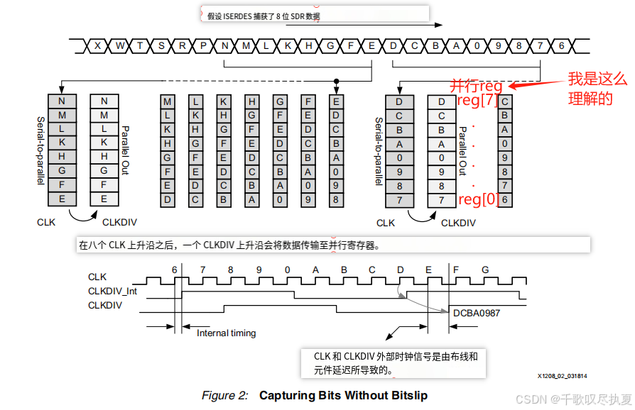
??????圖 2(SDR 操作)顯示了一個功能示例。數據采集??從位值 7 開始。位以 CLK 時鐘速率移入串并寄存器。垂直堆疊的塊代表該寄存器。這些塊顯示值為 7 的位首先移入,然后移至底部。最后移入的位是值為 D 的位。當串并寄存器包含八個采集位時,內部寄存器會采集其中的內容。在下一個 CLKDIV 上升沿,內容移至并行輸出寄存器。該寄存器隨后包含值 DCBA0987。
(不是你屏幕長蚊子了,是我翻譯貼圖了😹)
??????一旦數據從串行到并行寄存器被轉移到內部存儲寄存器,連續的新數據就被轉移到串行到并行寄存器中。
??????當使用Bitslip功能時,捕獲、傳輸到內部寄存器和傳輸到輸出寄存器的操作方式相同。
??????當ISERDES位滑輸入信號被斷言時,在串行到并行寄存器和內部寄存器之間的數據傳輸延遲一個CLK周期。
??????當數據傳輸延遲一個CLK周期時,一個額外的位被移到串行-并行寄存器中,另一端丟失一個位。
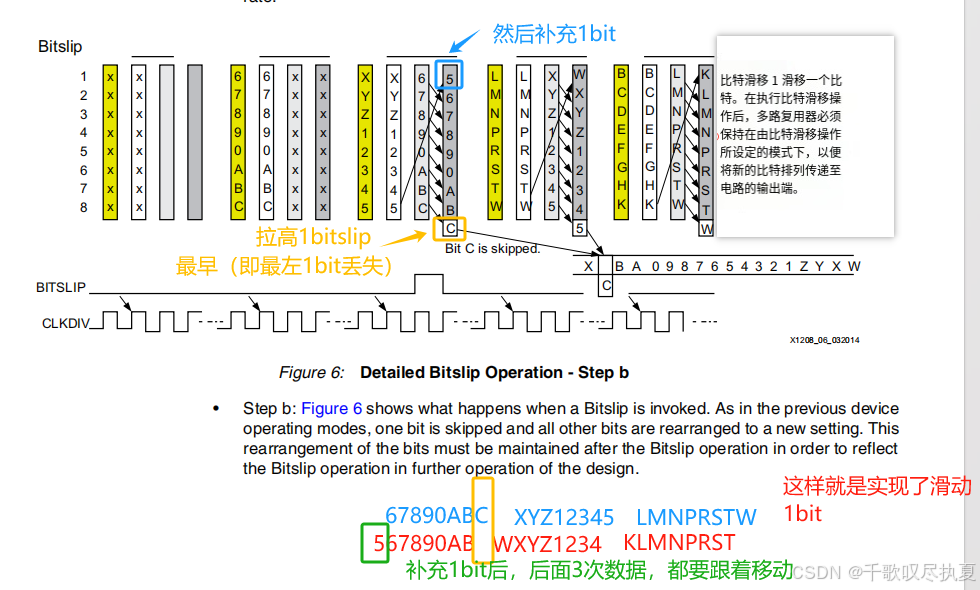
當數據在內部寄存器中被捕獲時,看起來好像數據被移動了一位。圖3顯示了與圖2相同的行為,除了在串行到并行寄存器中捕獲第二個字節時執行Bitslip操作。數據不是在捕獲第8位之后傳輸到并行寄存器,而是在捕獲第9位之后。看起來好像圖案移動了一位。在串行-并行寄存器的底部(末尾),移位的第一個位丟失。
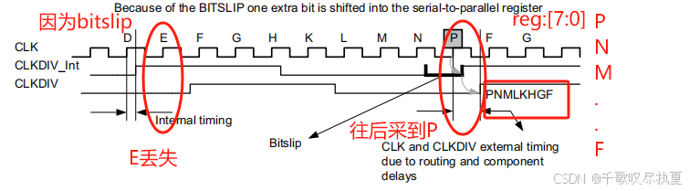
??????每次BITSLIP輸入保持高位超過半個CLKDIV周期,就對數據執行一次BITSLIP操作。連續捕獲相同的輸入位模式會導致位的移位。因此,這種機制可以很容易地用于將數據與模式對齊,或將一個數據通道與另一個數據通道對齊。
??????Bitslip 功能也可以在 I/O 邏輯的輸出端使用通用互連來實現。這意味著該功能必須對并行反序列化數據執行,而不是像在先前架構中(7系列FPGA)的原生 Bitslip 功能中解釋的那樣,對輸入的串行數據執行。
??????本文提供了一種電路,可以以 CLKDIV 速率對并行數據字中的位進行 Bitslip 或移位。可以構建幾種可能的電路來執行此操作。
2.3、解決方案A
??????現在介紹一種動態移位和預定移位解決方案。
??????以CLKDIV速率旋轉串行順序并行寄存器中的位。為了在所有可能性中進行位滑或移位,它將占用與寄存器寬度一樣多的CLKDIV時鐘周期
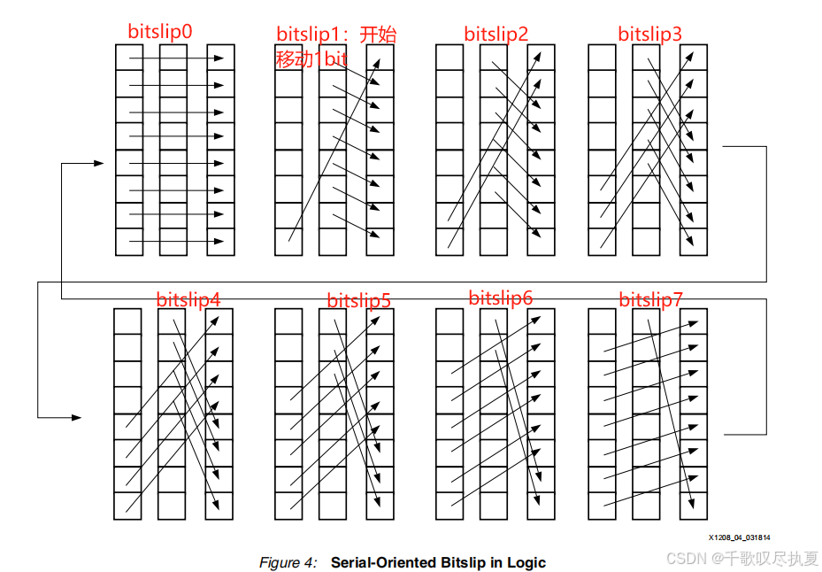
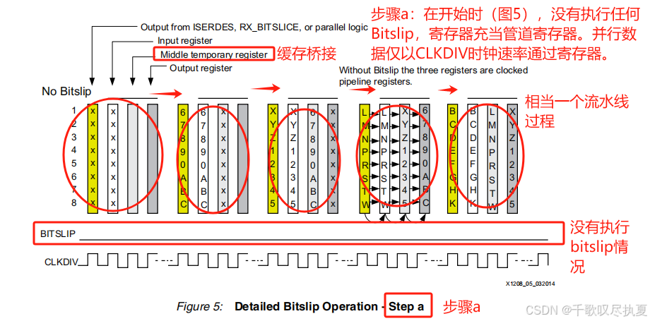
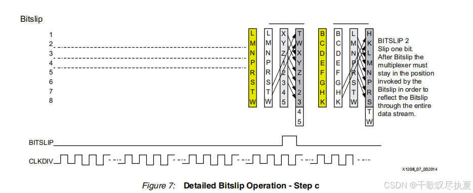
??????圖4顯示了8位字上所有可能的移位或位滑步。要執行這些操作,至少需要兩個8位寄存器和一個多路復用器。圖5到圖7詳細顯示了當執行單個Bitslip步驟時發生的情況。
覺得下面這個圖抽象不好理解的,可以結合2.2節第二個圖理解。
Step C,原理跟上面Step B一樣,只不過每次可以滑動2bit。
布局布線后框圖:
2.4、解決方案B
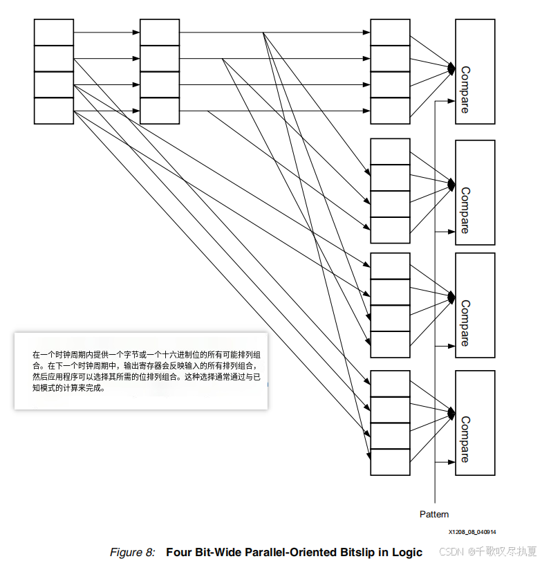
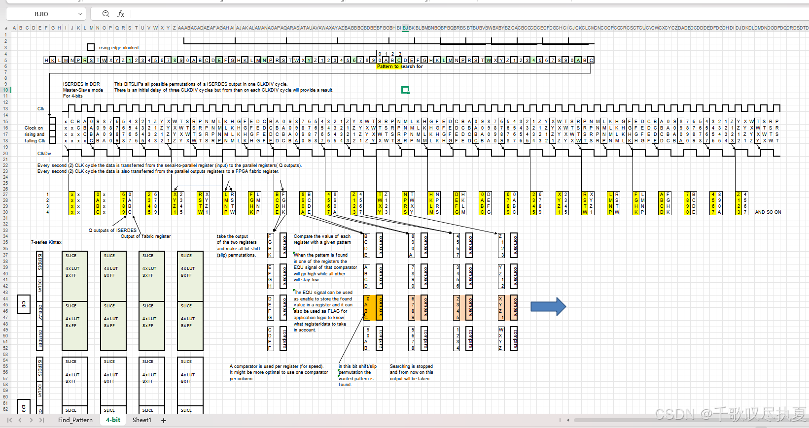
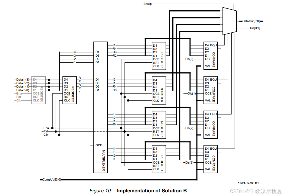
??????獲取ISERDES、RX_BITSLICE或其他并行邏輯的輸出,并將所有位同時旋轉到一組并行放置的寄存器中。該解決方案需要一個CLKDIV循環來遍歷所有可能的值。在操作開始時,需要兩個時鐘周期來獲得有效的輸出:一個初始時鐘周期用于加載歷史寄存器,第二個時鐘周期用于加載輸出寄存器中的所有位排列。從那時起,每個時鐘周期都會產生有效的輸出數據。然后,應用程序可以選擇具有所需位排列的小塊或字節。當必須檢測和匹配預先確定的模式時,此解決方案是理想的(參見圖8)。
框圖與代碼(2.4.1小節)的對應關系
從框圖中可以看到:
左側的4個方塊對應代碼中的輸入寄存器(IntRankOne)
中間的4個方塊對應位移寄存器(IntRankTwo)和位移邏輯
右側的多組寄存器和比較器對應于多種位移配置
"Compare"模塊對應于代碼中的比較邏輯
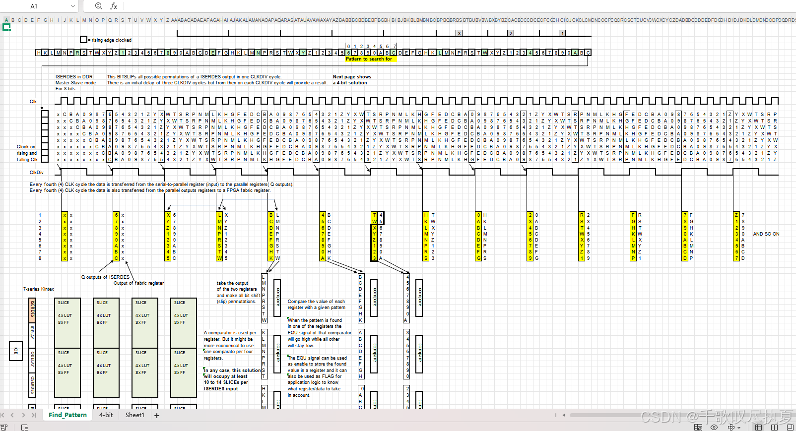
這個表格,就是上面框架圖4bit的。
整個代碼框架:
┌─────────────┐    ┌─────────────┐    ┌─────────────┐    ┌─────────────┐
│  輸入數據    │    │  位移邏輯   │    │ 比較與選擇  │     │    輸出      │
│ DataIn_pin  │───?│生成所有排列  │───?│ 根據模式選擇│───? │ DataOut_pin │
└─────────────┘    └─────────────┘    └─────────────┘    └─────────────┘│                  ▲                   ▲│                  │                   ││            ┌─────────────┐    ┌─────────────┐└───────────?│ 控制邏輯     │    │ 比較模式     ││ (模式選擇)   │?───│ CompVal_pin │└─────────────┘    └─────────────┘
雙緩沖寄存器結構框架:
┌───────────┐       ┌───────────┐       ┌───────────┐
│ IntRankOne│       │ IntRankTwo│       │ IntRankTre│
│ 當前輸入   │──────?│ 前一周期  │──────?│  輸出寄存  │
└───────────┘       └───────────┘       └───────────┘│                    │                   ▲│                    │                   │└────────┬───────────┘                   │▼                               │┌───────────────────────┐                ││     位移多路復用器     │                ││  (組合邏輯電路)     │────────────────┘└───────────────────────┘
2.4.1、8B verilog代碼:
`timescale 1ns / 1psmodule BitSlipInLogic_8b #(parameter C_Function  = "Slip",  // Slip, Nmbr, Compparameter C_ErrOut    = 1,       // 1 = ErrOut pin available.parameter C_InputReg  = 0        // 0, No, 1 = Yes
) (input  wire [7:0] DataIn_pin,input  wire       Bitslip_pin,input  wire [2:0] SlipVal_pin,input  wire [7:0] CompVal_pin,input  wire       Ena_pin,input  wire       Rst_pin,input  wire       Clk_pin,output wire [7:0] DataOut_pin,output wire       ErrOut_pin
);// Constants
localparam Low  = 1'b0;
localparam High = 1'b1;// Signals
reg  [7:0] IntBitSlipPosition;
reg        IntFrstBitSlipPstn;
reg  [7:0] IntBitSlipData;
wire [7:0] IntRankOne;
reg  [7:0] IntRankTwo;
reg  [7:0] IntRankTre;
wire       IntEnaReg;
reg        IntEnaReg_d;
wire       IntShftSlipReg;
reg        IntSlipPulse_d;
reg        IntShiftEna_d;
wire       IntSlipPulse;
wire       IntShiftEna;
wire       IntShftCntTc;
wire       IntShftCntEna;
wire       IntCompEqu;
reg        IntCompEqu_d;
wire       IntCompEqu_Rst;
wire       IntShftCntRst;
wire [2:0] IntBitSlipCntOut;
wire       IntErrOut;
reg        IntErrOut_d;// Attributes
(* KEEP_HIERARCHY = "YES" *) wire _unused_;
// Extra front input register.
// Adds one pipeline stage!

generateif (C_InputReg == 1) begin : Gen_1_0reg [7:0] IntRankOne_reg;always @(posedge Clk_pin or posedge Rst_pin) beginif (Rst_pin) IntRankOne_reg <= 8'b00000000;else if (Ena_pin)IntRankOne_reg <= DataIn_pin;endassign IntRankOne = IntRankOne_reg;end else begin : Gen_1_1assign IntRankOne = DataIn_pin;end
endgenerate
// These are the bitslip registers.

always @(posedge Clk_pin or posedge Rst_pin) beginif (Rst_pin) beginIntRankTwo <= 8'b00000000;IntRankTre <= 8'b00000000;end else beginif (Ena_pin)IntRankTwo <= IntRankOne;if (IntEnaReg)IntRankTre <= IntBitSlipData;end
endassign DataOut_pin = IntRankTre;// Mux logic for bit slipping
always @(*) begincase({Ena_pin, IntBitSlipPosition})9'b100000000: IntBitSlipData = IntRankOne[7:0];9'b100000001: IntBitSlipData = {IntRankOne[0], IntRankTwo[7:1]};9'b100000010: IntBitSlipData = {IntRankOne[1:0], IntRankTwo[7:2]};9'b100000100: IntBitSlipData = {IntRankOne[2:0], IntRankTwo[7:3]};9'b100001000: IntBitSlipData = {IntRankOne[3:0], IntRankTwo[7:4]};9'b100010000: IntBitSlipData = {IntRankOne[4:0], IntRankTwo[7:5]};9'b100100000: IntBitSlipData = {IntRankOne[5:0], IntRankTwo[7:6]};9'b101000000: IntBitSlipData = {IntRankOne[6:0], IntRankTwo[7]};9'b110000000: IntBitSlipData = IntRankOne[7:0];default:      IntBitSlipData = 8'b00000000;endcase
end
// This is the bitslip controller.
// When the attribute is set to "Slip" the generated controller is simple.
// When the attribute is set to "Nmbr" the controller is more complex.

always @(posedge Clk_pin or posedge Rst_pin) beginif (Rst_pin) beginIntBitSlipPosition <= 8'b00000000;IntFrstBitSlipPstn <= 1'b0;end else if (Ena_pin) beginif (IntShftSlipReg && !IntFrstBitSlipPstn)IntBitSlipPosition <= {IntBitSlipPosition[6:0], ~IntBitSlipPosition[7]};else if (IntShftSlipReg && IntFrstBitSlipPstn)IntBitSlipPosition <= {IntBitSlipPosition[6:0], IntBitSlipPosition[7]};if (IntShftSlipReg)IntFrstBitSlipPstn <= High;end
end
// Function specific logic

// "Slip" mode
generateif (C_Function == "Slip") begin : Gen_3assign IntShftSlipReg = Bitslip_pin;assign IntEnaReg = High;if (C_ErrOut == 0) begin : Gen_3_0assign ErrOut_pin = Low;end else begin : Gen_3_1// Got eight bitslips and the value is still not discovered.C3BCEtc C3BCEtc_inst (.CntClk(Clk_pin),.CntRst(Rst_pin),.CntEna(Bitslip_pin),.CntOut(),.CntTc(IntErrOut));FDCE #(.INIT(1'b0)) FDCE_ErrCntTc (.D(IntErrOut),.CE(Bitslip_pin),.C(Clk_pin),.CLR(Rst_pin),.Q(IntErrOut_d));GenPulse GenPulse_ErrCntTc (.Clk(Clk_pin),.Ena(High),.SigIn(IntErrOut_d),.SigOut(ErrOut_pin));endend// "Nmbr" modeelse if (C_Function == "Nmbr") begin : Gen_4always @(posedge Clk_pin or posedge Rst_pin) beginif (Rst_pin)IntSlipPulse_d <= 1'b0;else if (Ena_pin)IntSlipPulse_d <= Bitslip_pin;endalways @(posedge Clk_pin) beginif (Rst_pin || Bitslip_pin)IntEnaReg_d <= 1'b0;else if (IntShftCntTc)IntEnaReg_d <= High;endalways @(posedge Clk_pin) beginif (IntShftCntTc || Rst_pin)IntShiftEna_d <= 1'b0;else if (IntSlipPulse)IntShiftEna_d <= High;endassign IntSlipPulse = ~Bitslip_pin & IntSlipPulse_d;assign IntShiftEna = IntShiftEna_d | IntSlipPulse;assign IntShftCntEna = IntShiftEna & Ena_pin;assign IntShftSlipReg = IntShiftEna;assign IntEnaReg = IntShftCntTc | IntEnaReg_d;if (C_ErrOut == 0) begin : Gen_4_1assign ErrOut_pin = Low;end else begin : Gen_4_2FDCE #(.INIT(1'b0)) FDCE_CntTc (.D(IntShftCntTc),.CE(High),.C(Clk_pin),.CLR(Rst_pin),.Q(IntErrOut));assign ErrOut_pin = IntErrOut;endC3BCEtc_dwnld C3BCEtc_dwnld_inst (.CntClk(Clk_pin),.CntRst(IntShftCntRst),.CntEna(IntShftCntEna),.CntLoad(Bitslip_pin),.CntLdVal(SlipVal_pin),.CntOut(IntBitSlipCntOut),.CntTc(IntShftCntTc));GenPulse GenPulse_inst (.Clk(Clk_pin),.Ena(High),.SigIn(IntShftCntTc),.SigOut(IntShftCntRst));end// "Comp" modeelse if (C_Function == "Comp") begin : Gen_5assign IntShftSlipReg = Bitslip_pin;// Compare bit slipped data with the input data.assign IntCompEqu = (IntBitSlipData == CompVal_pin) ? 1'b1 : 1'b0;assign IntEnaReg = IntCompEqu | IntCompEqu_d;assign IntCompEqu_Rst = Rst_pin | Bitslip_pin;always @(posedge Clk_pin or posedge IntCompEqu_Rst) beginif (IntCompEqu_Rst)IntCompEqu_d <= 1'b0;else if (IntCompEqu)IntCompEqu_d <= High;endif (C_ErrOut == 0) begin : Gen_5_1assign ErrOut_pin = Low;end else begin : Gen_5_2FDCE #(.INIT(1'b0)) FDCE_ErrOut (.D(IntCompEqu),.CE(High),.C(Clk_pin),.CLR(Rst_pin),.Q(ErrOut_pin));endend
endgenerateendmodule//
// Helper Modules - Required by BitSlipInLogic_8b
//// C3BCEtc module - 3-bit binary counter with terminal count
module C3BCEtc (input  wire       CntClk,input  wire       CntRst,input  wire       CntEna,output wire [2:0] CntOut,output wire       CntTc
);reg [2:0] count;always @(posedge CntClk or posedge CntRst) beginif (CntRst)count <= 3'b000;else if (CntEna)count <= count + 1'b1;endassign CntOut = count;assign CntTc = (count == 3'b111) & CntEna;
endmodule// C3BCEtc_dwnld module - 3-bit binary counter with terminal count and load capability
module C3BCEtc_dwnld (input  wire       CntClk,input  wire       CntRst,input  wire       CntEna,input  wire       CntLoad,input  wire [2:0] CntLdVal,output wire [2:0] CntOut,output wire       CntTc
);reg [2:0] count;always @(posedge CntClk or posedge CntRst) beginif (CntRst)count <= 3'b000;else if (CntLoad)count <= CntLdVal;else if (CntEna)count <= count + 1'b1;endassign CntOut = count;assign CntTc = (count == 3'b111) & CntEna;
endmodule// GenPulse module - Generates a single clock pulse
module GenPulse (input  wire Clk,input  wire Ena,input  wire SigIn,output wire SigOut
);reg sig_d;always @(posedge Clk) beginif (Ena)sig_d <= SigIn;endassign SigOut = SigIn & ~sig_d & Ena;
endmodule
2.4.2、分析一下代碼
代碼中有三種工作模式,每種模式下比較和位移的實現略有不同:
- "Slip"模式:
最簡單的模式,位移操作由外部信號Bitslip_pin直接控制
每次Bitslip_pin為高時,執行一次位移操作
輸出寄存器始終啟用(IntEnaReg = High) - "Nmbr"模式:
更復雜的模式,使用計數器控制位移次數
可以通過SlipVal_pin設置特定的位移次數
使用下降沿檢測生成位移脈沖 - "Comp"模式:
自動搜索匹配模式的模式
對每種位移配置進行比較,直到找到與CompVal_pin匹配的排列
找到匹配后,停止位移并保持輸出穩定
在"Comp"模式下,位移操作由比較結果自動控制:
else if (C_Function == "Comp") begin : Gen_5assign IntShftSlipReg = Bitslip_pin;// Compare bit slipped data with the input data.assign IntCompEqu = (IntBitSlipData == CompVal_pin) ? 1'b1 : 1'b0;assign IntEnaReg = IntCompEqu | IntCompEqu_d;assign IntCompEqu_Rst = Rst_pin | Bitslip_pin;// ...
end
這是一個純組合邏輯電路,不需要時鐘信號,可以在一個時鐘周期內完成所有可能組合的計算。它基于當前的位移位置(IntBitSlipPosition)從兩個寄存器(IntRankOne和IntRankTwo)中選擇適當的位來組成新的8位數據。
always @(*) begincase({Ena_pin, IntBitSlipPosition})9'b100000000: IntBitSlipData = IntRankOne[7:0];9'b100000001: IntBitSlipData = {IntRankOne[0], IntRankTwo[7:1]};9'b100000010: IntBitSlipData = {IntRankOne[1:0], IntRankTwo[7:2]};9'b100000100: IntBitSlipData = {IntRankOne[2:0], IntRankTwo[7:3]};9'b100001000: IntBitSlipData = {IntRankOne[3:0], IntRankTwo[7:4]};9'b100010000: IntBitSlipData = {IntRankOne[4:0], IntRankTwo[7:5]};9'b100100000: IntBitSlipData = {IntRankOne[5:0], IntRankTwo[7:6]};9'b101000000: IntBitSlipData = {IntRankOne[6:0], IntRankTwo[7]};9'b110000000: IntBitSlipData = IntRankOne[7:0];default:      IntBitSlipData = 8'b00000000;endcase
end
畫一下狀態轉移圖,方便大家理解:
假設:
IntRankOne (當前數據) = [A7][A6][A5][A4][A3][A2][A1][A0]
IntRankTwo (前一周期數據) = [B7][B6][B5][B4][B3][B2][B1][B0]
位移位置 0 (IntBitSlipPosition = 00000000, 初始或復位狀態):
+---+---+---+---+---+---+---+---+
| A7| A6| A5| A4| A3| A2| A1| A0|  IntRankOne[7:0]
+---+---+---+---+---+---+---+---+|   |   |   |   |   |   |   |v   v   v   v   v   v   v   v
+---+---+---+---+---+---+---+---+
| A7| A6| A5| A4| A3| A2| A1| A0|  IntBitSlipData
+---+---+---+---+---+---+---+---+位移位置 1 (IntBitSlipPosition = 00000001, 第一次位移):
+---+    +---+---+---+---+---+---+---+
| A0|    | B7| B6| B5| B4| B3| B2| B1|
+---+    +---+---+---+---+---+---+---+|        |   |   |   |   |   |   |v        v   v   v   v   v   v   v
+---+---+---+---+---+---+---+---+
| A0| B7| B6| B5| B4| B3| B2| B1|  IntBitSlipData
+---+---+---+---+---+---+---+---+位移位置 2 (IntBitSlipPosition = 00000010, 第二次位移):
+---+---+    +---+---+---+---+---+---+
| A1| A0|    | B7| B6| B5| B4| B3| B2|
+---+---+    +---+---+---+---+---+---+|   |        |   |   |   |   |   |v   v        v   v   v   v   v   v
+---+---+---+---+---+---+---+---+
| A1| A0| B7| B6| B5| B4| B3| B2|  IntBitSlipData
+---+---+---+---+---+---+---+---+位移位置 3 (IntBitSlipPosition = 00000100, 第三次位移):
+---+---+---+    +---+---+---+---+---+
| A2| A1| A0|    | B7| B6| B5| B4| B3|
+---+---+---+    +---+---+---+---+---+|   |   |        |   |   |   |   |v   v   v        v   v   v   v   v
+---+---+---+---+---+---+---+---+
| A2| A1| A0| B7| B6| B5| B4| B3|  IntBitSlipData
+---+---+---+---+---+---+---+---+位移位置 4 (IntBitSlipPosition = 00001000, 第四次位移):
+---+---+---+---+    +---+---+---+---+
| A3| A2| A1| A0|    | B7| B6| B5| B4|
+---+---+---+---+    +---+---+---+---+|   |   |   |        |   |   |   |v   v   v   v        v   v   v   v
+---+---+---+---+---+---+---+---+
| A3| A2| A1| A0| B7| B6| B5| B4|  IntBitSlipData
+---+---+---+---+---+---+---+---+位移位置 5 (IntBitSlipPosition = 00010000, 第五次位移):
+---+---+---+---+---+    +---+---+---+
| A4| A3| A2| A1| A0|    | B7| B6| B5|
+---+---+---+---+---+    +---+---+---+|   |   |   |   |        |   |   |v   v   v   v   v        v   v   v
+---+---+---+---+---+---+---+---+
| A4| A3| A2| A1| A0| B7| B6| B5|  IntBitSlipData
+---+---+---+---+---+---+---+---+位移位置 6 (IntBitSlipPosition = 00100000, 第六次位移):
+---+---+---+---+---+---+    +---+---+
| A5| A4| A3| A2| A1| A0|    | B7| B6|
+---+---+---+---+---+---+    +---+---+|   |   |   |   |   |        |   |v   v   v   v   v   v        v   v
+---+---+---+---+---+---+---+---+
| A5| A4| A3| A2| A1| A0| B7| B6|  IntBitSlipData
+---+---+---+---+---+---+---+---+位移位置 7 (IntBitSlipPosition = 01000000, 第七次位移):
+---+---+---+---+---+---+---+    +---+
| A6| A5| A4| A3| A2| A1| A0|    | B7|
+---+---+---+---+---+---+---+    +---+|   |   |   |   |   |   |        |v   v   v   v   v   v   v        v
+---+---+---+---+---+---+---+---+
| A6| A5| A4| A3| A2| A1| A0| B7|  IntBitSlipData
+---+---+---+---+---+---+---+---+位移位置 8 (IntBitSlipPosition = 10000000, 第八次位移):
+---+---+---+---+---+---+---+---+
| A7| A6| A5| A4| A3| A2| A1| A0|  IntRankOne[7:0]
+---+---+---+---+---+---+---+---+|   |   |   |   |   |   |   |v   v   v   v   v   v   v   v
+---+---+---+---+---+---+---+---+
| A7| A6| A5| A4| A3| A2| A1| A0|  IntBitSlipData (與位置0相同)
+---+---+---+---+---+---+---+---+
"Comp"模式在找到匹配后不會自動停止位移操作,位移操作完全由外部Bitslip_pin信號控制。然而,它會自動鎖定輸出為匹配的配置,這是通過IntCompEqu_d寄存器和輸出使能邏輯實現的。需要結合自己代碼實現training。
布局布線后的框圖:
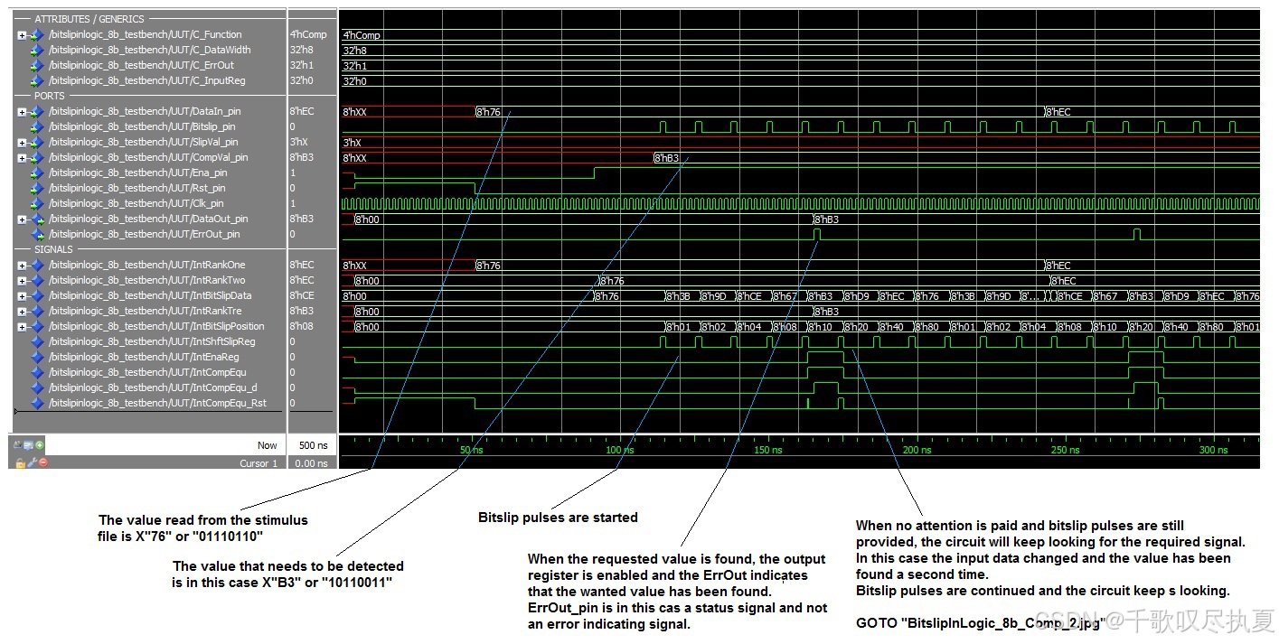
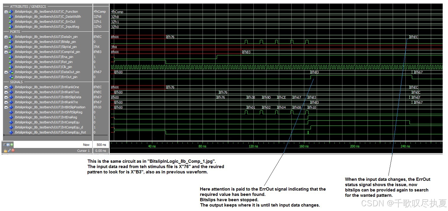
??????0x76,需要找到0xB3,不停bitslip知道找到0xB3。找到0xB3后,ErrOut_pin拉高,可以從代碼看:assign IntCompEqu = (IntBitSlipData == CompVal_pin) ? 1’b1 : 1’b0;
參考設計包含上述兩種電路,所選的選項決定了所使用的電路和選項。參考設計是一個可實例化的組件,包含一組可選選項。兩種可能的電路各自使用一組選項來應用設計特性。
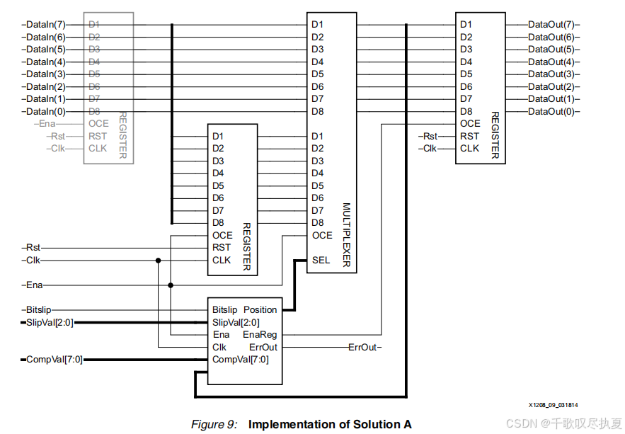
參考設計組件如圖 1 所示。引腳功能如下:
? DataIn:4 位或 8 位輸入。在 4 位模式下,使用 LSB 半字節。
? BitSlip:控制輸入,當脈沖為高電平時,將調用解決方案 A 的 Bitslip 和解決方案 B 的電路使能。
? SlipVal:3 位輸入,允許電路在使能輸出之前進行定義的 Bitslip 次數。
? CompVal:8 位輸入,用于檢測數據中的模式。在 4 位模式下,使用 LSB 半字節。
? Ena:電路使能,高電平有效。
? Rst:電路復位,高電平有效。
? Clk:時鐘,通常等于 CLKDIV 時鐘。
? DataOut:4 位或 8 位輸出。在 4 位模式下,使用 LSB 半字節。
? ErrOut:錯誤和狀態輸出:
? “Slip” 模式:執行 8 個 Bitslip 后輸出高電平脈沖。
? “Nmbr” 模式:表示在執行“Nmbr”個 Bitslip 后輸出數據已準備就緒。
? “Comp” 模式:表示檢測到請求的模式。
3、RX_BITSLICE功能
補充個概念:
??????討論UltraScale(UltraScale+) IO,那就避不開RX_BITSLICE。
??????在Ultrascale (plus即+)系列上的FPGA中,Xilinx引入了bitslice硬核,它取代了7系列上的IDELAYCTRL/IODELAY/IOSERDES/IODDR系列硬核,用于為HP(High Performance)類型Bank上的IO接口提供串并轉化、信號延時、三態控制等功能。Xilinx為bitslice硬核提供了TXRX_BITSLICE/TX_BITSLICE/RX_BITSLICE/BITSLICE_CONTROL/TX_BITSLICE_TRI/RIU_OR??????這些與bitslice硬核接口一致的原生原語便于用戶直接調用例化。同時為了提供向前兼容性,IDELAYCTRL/IODELAY/IOSERDES/IODDR系列原語作為組件原語仍能繼續使用,在綜合時會被軟件綜合為bitslice。
??????使用bitslice原生原語的優勢在于其能夠對位于一個字節組上的接口進行批量控制,這對于存儲控制器(如DDR)的接口信號時序的優化十分有效。此外bitslice在接收側增加了一個異步FIFO,便于用戶邏輯通過用戶時鐘讀取數據。
??????官方手冊是這樣解釋功能的:
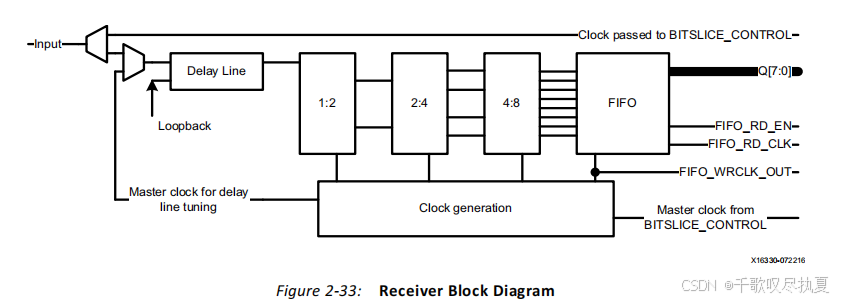
??????在本機模式下,RX_BITSLICE包含反序列化邏輯和512分接輸入延遲(iddelay),可以連續調整VT變化(這個類似之前的IDELAYCTRL)。RX_BITSLICE包含用于1:4或1:8反序列化的反序列化邏輯,以及允許連接到另一個時鐘域的淺FIFO。

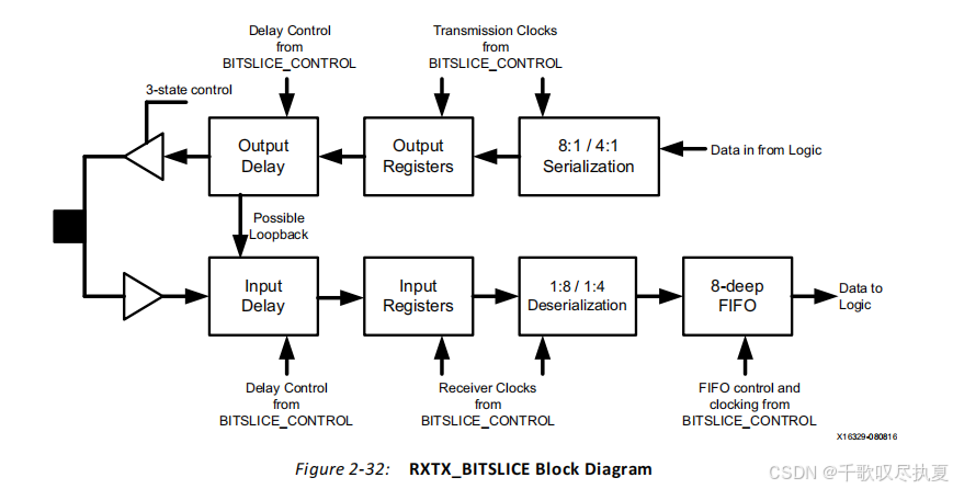
RX_BITSLICE模塊結構圖:


管腳信號,這里就不寫了,自己看看ug974。
// RX_BITSLICE : In order to incorporate this function into the design,
//   Verilog   : the following instance declaration needs to be placed
//  instance   : in the body of the design code.  The instance name
// declaration : (RX_BITSLICE_inst) and/or the port declarations within the
//    code     : parenthesis may be changed to properly reference and
//             : connect this function to the design.  All inputs
//             : and outputs must be connected.//  <-----Cut code below this line---->// RX_BITSLICE: RX_BITSLICE for input using Native Mode//              Kintex UltraScale// Xilinx HDL Language Template, version 2022.2RX_BITSLICE #(.CASCADE("FALSE"),              // Enables cascading of IDELAY and ODELAY lines.DATA_TYPE("DATA"),             // Defines what the input pin is carrying (CLOCK, DATA, DATA_AND_CLOCK,// SERIAL).DATA_WIDTH(8),                 // Defines the width of the serial-to-parallel converter (4-8).DELAY_FORMAT("TIME"),          // Units of the DELAY_VALUE (COUNT, TIME).DELAY_TYPE("FIXED"),           // Set the type of tap delay line (FIXED, VARIABLE, VAR_LOAD).DELAY_VALUE(0),                // Input delay value setting in ps.DELAY_VALUE_EXT(0),            // Value of the extended input delay value in ps.FIFO_SYNC_MODE("FALSE"),       // Always set to FALSE. TRUE is reserved for later use..IS_CLK_EXT_INVERTED(1'b0),     // Optional inversion for CLK_EXT.IS_CLK_INVERTED(1'b0),         // Optional inversion for CLK.IS_RST_DLY_EXT_INVERTED(1'b0), // Optional inversion for RST_DLY_EXT.IS_RST_DLY_INVERTED(1'b0),     // Optional inversion for RST_DLY.IS_RST_INVERTED(1'b0),         // Optional inversion for RST.REFCLK_FREQUENCY(300.0),       // Specification of the reference clock frequency in MHz (200.0-2667.0).SIM_DEVICE("ULTRASCALE"),      // Set the device version for simulation functionality (ULTRASCALE).UPDATE_MODE("ASYNC"),          // Determines when updates to the delay will take effect (ASYNC, MANUAL,// SYNC).UPDATE_MODE_EXT("ASYNC")       // Determines when updates to the extended input delay will take effect// (ASYNC, MANUAL, SYNC))RX_BITSLICE_inst (.CNTVALUEOUT(CNTVALUEOUT),         // 9-bit output: Counter value to device logic.CNTVALUEOUT_EXT(CNTVALUEOUT_EXT), // 9-bit output: Optional extended (cascaded delay) counter value// going to the device logic.FIFO_EMPTY(FIFO_EMPTY),           // 1-bit output: FIFO empty flag.FIFO_WRCLK_OUT(FIFO_WRCLK_OUT),   // 1-bit output: FIFO source synchronous write clock out to the device// logic (currently unsupported, do not connect).Q(Q),                             // 8-bit output: Registered output data from FIFO.RX_BIT_CTRL_OUT(RX_BIT_CTRL_OUT), // 40-bit output: Output bus to BITSLICE_CONTROL.TX_BIT_CTRL_OUT(TX_BIT_CTRL_OUT), // 40-bit output: Output bus to BITSLICE_CONTROL.CE(CE),                           // 1-bit input: Clock enable for IDELAY.CE_EXT(CE_EXT),                   // 1-bit input: Optional extended (cascaded delay) clock enable.CLK(CLK),                         // 1-bit input: Clock used to sample LOAD, CE, INC.CLK_EXT(CLK_EXT),                 // 1-bit input: Optional extended (cascaded delay) clock.CNTVALUEIN(CNTVALUEIN),           // 9-bit input: Counter value from device logic.CNTVALUEIN_EXT(CNTVALUEIN_EXT),   // 9-bit input: Optional extended (cascaded delay) counter value from// device logic.DATAIN(DATAIN),                   // 1-bit input: Input signal from IBUF.EN_VTC(EN_VTC),                   // 1-bit input: Enable IDELAYCTRL to keep stable delay over VT.EN_VTC_EXT(EN_VTC_EXT),           // 1-bit input: Optional extended (cascaded delay) to keep stable// delay over VT.FIFO_RD_CLK(FIFO_RD_CLK),         // 1-bit input: FIFO read clock.FIFO_RD_EN(FIFO_RD_EN),           // 1-bit input: FIFO read enable.INC(INC),                         // 1-bit input: Increment the current delay tap setting.INC_EXT(INC_EXT),                 // 1-bit input: Optional extended (cascaded delay) increments the// current delay tap setting.LOAD(LOAD),                       // 1-bit input: Load the CNTVALUEIN tap setting.LOAD_EXT(LOAD_EXT),               // 1-bit input: Optional extended (cascaded delay) load the// CNTVALUEIN_EXT tap setting.RST(RST),                         // 1-bit input: Asynchronous assert, synchronous deassert for// RX_BITSLICE ISERDES.RST_DLY(RST_DLY),                 // 1-bit input: Reset the internal DELAY value to DELAY_VALUE.RST_DLY_EXT(RST_DLY_EXT),         // 1-bit input: Optional extended (cascaded delay) reset delay to// DELAY_VALUE_EXT.RX_BIT_CTRL_IN(RX_BIT_CTRL_IN),   // 40-bit input: Input bus from BITSLICE_CONTROL.TX_BIT_CTRL_IN(TX_BIT_CTRL_IN)    // 40-bit input: Input bus from BITSLICE_CONTROL);// End of RX_BITSLICE_inst instantiation
RXTX_BITSLICE模塊結構圖:
除了接收,也有發送或者雙向的同樣模塊:RXTX_BITSLICE。
功能類似,這里不贅述。
// RXTX_BITSLICE : In order to incorporate this function into the design,
//    Verilog    : the following instance declaration needs to be placed
//   instance    : in the body of the design code.  The instance name
//  declaration  : (RXTX_BITSLICE_inst) and/or the port declarations within the
//     code      : parenthesis may be changed to properly reference and
//               : connect this function to the design.  All inputs
//               : and outputs must be connected.//  <-----Cut code below this line---->// RXTX_BITSLICE: RXTX_BITSLICE for bidirectional I/O using Native Mode//                Kintex UltraScale// Xilinx HDL Language Template, version 2022.2RXTX_BITSLICE #(.ENABLE_PRE_EMPHASIS("FALSE"), // Enable the pre-emphasis.FIFO_SYNC_MODE("FALSE"),      // Always set to FALSE. TRUE is reserved for later use..INIT(1'b1),                   // Defines initial O value.IS_RX_CLK_INVERTED(1'b0),     // Optional inversion for RX_CLK.IS_RX_RST_DLY_INVERTED(1'b0), // Optional inversion for RX_RST_DLY.IS_RX_RST_INVERTED(1'b0),     // Optional inversion for RX_RST.IS_TX_CLK_INVERTED(1'b0),     // Optional inversion for TX_CLK.IS_TX_RST_DLY_INVERTED(1'b0), // Optional inversion for TX_RST_DLY.IS_TX_RST_INVERTED(1'b0),     // Optional inversion for TX_RST.RX_DATA_TYPE("DATA"),         // Defines what the RX input pin is carrying (CLOCK, DATA, DATA_AND_CLOCK,// SERIAL).RX_DATA_WIDTH(8),             // Defines the width of the serial-to-parallel converter (4-8).RX_DELAY_FORMAT("TIME"),      // Units of the RX DELAY_VALUE (COUNT, TIME).RX_DELAY_TYPE("FIXED"),       // Set the type of RX tap delay line (FIXED, VARIABLE, VAR_LOAD).RX_DELAY_VALUE(0),            // RX Input delay value setting in ps.RX_REFCLK_FREQUENCY(300.0),   // Specification of the RX reference clock frequency in MHz (200.0-2667.0).RX_UPDATE_MODE("ASYNC"),      // Determines when updates to the RX delay will take effect (ASYNC,// MANUAL, SYNC).SIM_DEVICE("ULTRASCALE"),     // Set the device version for simulation functionality (ULTRASCALE).TBYTE_CTL("TBYTE_IN"),        // Select between T and TBYTE_IN inputs.TX_DATA_WIDTH(8),             // Parallel data input width (4-8).TX_DELAY_FORMAT("TIME"),      // Units of the TX DELAY_VALUE (COUNT, TIME).TX_DELAY_TYPE("FIXED"),       // Set the type of TX tap delay line (FIXED, VARIABLE, VAR_LOAD).TX_DELAY_VALUE(0),            // TX Input delay value setting in ps.TX_OUTPUT_PHASE_90("FALSE"),  // Delays the output phase by 90-degrees.TX_REFCLK_FREQUENCY(300.0),   // Specification of the TX reference clock frequency in MHz (200.0-2667.0).TX_UPDATE_MODE("ASYNC")       // Determines when updates to the delay will take effect (ASYNC, MANUAL,// SYNC))RXTX_BITSLICE_inst (.FIFO_EMPTY(FIFO_EMPTY),           // 1-bit output: FIFO empty flag.FIFO_WRCLK_OUT(FIFO_WRCLK_OUT),   // 1-bit output: FIFO source synchronous write clock out to the device// logic (currently unsupported, do not connect).O(O),                             // 1-bit output: Serialized output going to output buffer.Q(Q),                             // 8-bit output: Registered output data from FIFO.RX_BIT_CTRL_OUT(RX_BIT_CTRL_OUT), // 40-bit output: RX Output bus to BITSLICE_CONTROL.RX_CNTVALUEOUT(RX_CNTVALUEOUT),   // 9-bit output: RX Counter value from device logic.TX_BIT_CTRL_OUT(TX_BIT_CTRL_OUT), // 40-bit output: Output bus to BITSLICE_CONTROL for TX.TX_CNTVALUEOUT(TX_CNTVALUEOUT),   // 9-bit output: TX Counter value to device logic.T_OUT(T_OUT),                     // 1-bit output: Byte group 3-state output.D(D),                             // 8-bit input: Data from device logic.DATAIN(DATAIN),                   // 1-bit input: Input signal from IOBUF.FIFO_RD_CLK(FIFO_RD_CLK),         // 1-bit input: FIFO read clock.FIFO_RD_EN(FIFO_RD_EN),           // 1-bit input: FIFO read enable.RX_BIT_CTRL_IN(RX_BIT_CTRL_IN),   // 40-bit input: RX Input bus from BITSLICE_CONTROL.RX_CE(RX_CE),                     // 1-bit input: Clock enable for IDELAY.RX_CLK(RX_CLK),                   // 1-bit input: RX Clock used to sample LOAD, CE, INC.RX_CNTVALUEIN(RX_CNTVALUEIN),     // 9-bit input: RX Counter value from device logic.RX_EN_VTC(RX_EN_VTC),             // 1-bit input: RX Enable to keep stable delay over VT.RX_INC(RX_INC),                   // 1-bit input: RX Increment the current delay tap setting.RX_LOAD(RX_LOAD),                 // 1-bit input: RX Load the CNTVALUEIN tap setting.RX_RST(RX_RST),                   // 1-bit input: RX Asynchronous assert, synchronous deassert for// RXTX_BITSLICE ISERDES.RX_RST_DLY(RX_RST_DLY),           // 1-bit input: RX Reset the internal DELAY value to DELAY_VALUE.T(T),                             // 1-bit input: Legacy T byte input from device logic.TBYTE_IN(TBYTE_IN),               // 1-bit input: Byte group 3-state input from TX_BITSLICE_TRI.TX_BIT_CTRL_IN(TX_BIT_CTRL_IN),   // 40-bit input: TX Input bus from BITSLICE_CONTROL.TX_CE(TX_CE),                     // 1-bit input: Clock enable for ODELAY.TX_CLK(TX_CLK),                   // 1-bit input: TX Clock used to sample LOAD, CE, INC.TX_CNTVALUEIN(TX_CNTVALUEIN),     // 9-bit input: TX Counter value from device logic.TX_EN_VTC(TX_EN_VTC),             // 1-bit input: TX Enable to keep stable delay over VT.TX_INC(TX_INC),                   // 1-bit input: TX Increment the current delay tap setting.TX_LOAD(TX_LOAD),                 // 1-bit input: TX Load the CNTVALUEIN tap setting.TX_RST(TX_RST),                   // 1-bit input: TX Asynchronous assert, synchronous deassert for// RXTX_BITSLICE OSERDES.TX_RST_DLY(TX_RST_DLY)            // 1-bit input: TX Reset the internal DELAY value to DELAY_VALUE);// End of RXTX_BITSLICE_inst instantiation
4、工程獲取
4.1、部分代碼
????美中不足,xilinx參考代碼是VHD寫的,頂層文件BitSlipInLogic_Toplevel如下:
---------------------------------------------------------------------------------------------
--   ____  ____
--  /   /\/   /
-- /___/  \  /
-- \   \   \/    ?Copyright 2014 Xilinx, Inc. All rights reserved.
--  \   \        This file contains confidential and proprietary information of Xilinx, Inc.
--  /   /        and is protected under U.S. and international copyright and other
-- /___/   /\    intellectual property laws.
-- \   \  /  \
--  \___\/\___\
--
---------------------------------------------------------------------------------------------
-- Device:              UltraScale, 7-Series
-- Author:              Defossez
-- Entity Name:         BitSlipInLogic_Toplevel
-- Purpose:             Is same design as Bitslip.vhd but now with front and back-end
--                      registers added. These are added for software timing measurements.
--                      Perform bitslip operations on parallel data.
--                      Extended functionality of native Virtex and 7-Series bitslip.
-- Tools:               Vivado_2014.1 or newer
-- Limitations:         none
--
-- Vendor:              Xilinx Inc.
-- Version:             V0.01
-- Filename:            BitSlipInLogic_Toplevel.vhd
-- Date Created:        5 Dec 2014
-- Date Last Modified:  May 2014
---------------------------------------------------------------------------------------------
-- Disclaimer:
--		This disclaimer is not a license and does not grant any rights to the materials
--		distributed herewith. Except as otherwise provided in a valid license issued to you
--		by Xilinx, and to the maximum extent permitted by applicable law: (1) THESE MATERIALS
--		ARE MADE AVAILABLE "AS IS" AND WITH ALL FAULTS, AND XILINX HEREBY DISCLAIMS ALL
--		WARRANTIES AND CONDITIONS, EXPRESS, IMPLIED, OR STATUTORY, INCLUDING BUT NOT LIMITED
--		TO WARRANTIES OF MERCHANTABILITY, NON-INFRINGEMENT, OR FITNESS FOR ANY PARTICULAR
--		PURPOSE; and (2) Xilinx shall not be liable (whether in contract or tort, including
--		negligence, or under any other theory of liability) for any loss or damage of any
--		kind or nature related to, arising under or in connection with these materials,
--		including for any direct, or any indirect, special, incidental, or consequential
--		loss or damage (including loss of data, profits, goodwill, or any type of loss or
--		damage suffered as a result of any action brought by a third party) even if such
--		damage or loss was reasonably foreseeable or Xilinx had been advised of the
--		possibility of the same.
--
-- CRITICAL APPLICATIONS
--		Xilinx products are not designed or intended to be fail-safe, or for use in any
--		application requiring fail-safe performance, such as life-support or safety devices
--		or systems, Class III medical devices, nuclear facilities, applications related to
--		the deployment of airbags, or any other applications that could lead to death,
--		personal injury, or severe property or environmental damage (individually and
--		collectively, "Critical Applications"). Customer assumes the sole risk and
--		liability of any use of Xilinx products in Critical Applications, subject only to
--		applicable laws and regulations governing limitations on product liability.
--
-- THIS COPYRIGHT NOTICE AND DISCLAIMER MUST BE RETAINED AS PART OF THIS FILE AT ALL TIMES.
--
-- Contact:    e-mail  hotline@xilinx.com        phone   + 1 800 255 7778
---------------------------------------------------------------------------------------------
-- Revision History:
--  Rev. May 2014
--  Checked simulations and implementation.
--  Reorganise design to fit Olympus and UltraScale, 7-Series XiPhy / ISERDES.
---------------------------------------------------------------------------------------------
-- Naming Conventions:
--  Generics start with:                                    "C_*"
--  Ports
--      All words in the label of a port name start with a upper case, AnInputPort.
--      Active low ports end in                             "*_n"
--      Active high ports of a differential pair end in:    "*_p"
--      Ports being device pins end in _pin                 "*_pin"
--      Reset ports end in:                                 "*Rst"
--      Enable ports end in:                                "*Ena", "*En"
--      Clock ports end in:                                 "*Clk", "ClkDiv", "*Clk#"
--  Signals and constants
--      Signals and constant labels start with              "Int*"
--      Registered signals end in                           "_d#"
--      User defined types:                                 "*_TYPE"
--      State machine next state:                           "*_Ns"
--      State machine current state:                        "*_Cs"
--      Counter signals end in:                             "*Cnt", "*Cnt_n"
--   Processes:                                 "<Entity_><Function>_PROCESS"
--   Component instantiations:                  "<Entity>_I_<Component>_<Function>"
---------------------------------------------------------------------------------------------
library IEEE;use IEEE.std_logic_1164.all;use IEEE.std_logic_UNSIGNED.all;
library UNISIM;use UNISIM.vcomponents.all;
library work;use work.all;
library Common;use Common.all;
---------------------------------------------------------------------------------------------
-- Entity pin description
-- View also PDF documentation in the /Documents Folder
--  GENERICS / ATTRIBUTES
--  C_Function      :   "Slip" = Normal bitslip. One bit at a time when C_PulsedSlip is 1,
--                  :            else bitslip will happen as long as the BitSlip_Pin is high.
--                  :   "Nmbr" = Perform the given amount of bitslips.
--                  :   "Comp" = Compare. Auto bitslip until the given value is detected.
--                  :   "FstC" = Fast Compare. Different (Low latency) implementation of the
--                  :            compare bitslip solution.
--  C_DataWidth     :   8, 4
--  C_PulsedSlip    :   If set to 1, bitslip is reduced to a clock period.
--                  :   Leave this at '1', unless you are sure that bitslip given by an
--                  :   application is not longer than one Clk_pin cycle.
--  C_ErrOut        :   1 = ErrOut pin available.
--  C_InputReg      :   0 = No. Provide an extra input register for the module.
--
--  INPUT / OUTPUT PINS
--  DataIn_pin      :   in : Data input 4 or 8-bit wide.
--  Bitslip_pin     :   in : Perform bitslip when high
--  SlipVal_pin     :   in : Given number of bitslips. For 8-bit this is a 3-bit binary value.
--                  :        For 4-bit this is a 2-bit binary value (Pull MSB bit low)
--  CompVal_pin     :   in : Provided value to compare the input data against.
--  Ena_pin         :   in
--  Rst_pin         :   in
--  Clk_pin         :   in
--  DataOut_pin     :   out 4-bit or 8-bit output data.
--  ErrOut_pin      :   out Error or status depending on C_Function.
---------------------------------------------------------------------------------------------
entity BitSlipInLogic_Toplevel isgeneric (C_Function      : string    := "Comp";  -- Slip, Nmbr, Comp, FstCC_DataWidth     : integer   := 8;       -- 8, 4C_PulsedSlip    : integer   := 1;       -- 1 = bitslip is reduced to a clock period.-- Leave this at '1', unless you are sure that-- a bitslip given by an application is longer-- than one Clk_pin cycle.C_ErrOut        : integer   := 1;       -- 1 = ErrOut pin available.C_InputReg      : integer   := 0        -- 0, No, 1 = Yes);port (DataIn_pin      : in std_logic_vector(C_DataWidth-1 downto 0);Bitslip_pin     : in std_logic;SlipVal_pin     : in std_logic_vector(2 downto 0);CompVal_pin     : in std_logic_vector(C_DataWidth-1 downto 0);Ena_pin         : in std_logic;Rst_pin         : in std_logic;Clk_pin         : in std_logic;DataOut_pin     : out std_logic_vector(C_DataWidth-1 downto 0);ErrOut_pin      : out std_logic);
end BitSlipInLogic_Toplevel;
---------------------------------------------------------------------------------------------
-- Architecture section
---------------------------------------------------------------------------------------------
architecture BitSlipInLogic_Toplevel_arch of BitSlipInLogic_Toplevel is
---------------------------------------------------------------------------------------------
-- Component Instantiation
---------------------------------------------------------------------------------------------
---------------------------------------------------------------------------------------------
-- Constants, Signals and Attributes Declarations
---------------------------------------------------------------------------------------------
-- Functions
-- Constants
constant Low  : std_logic	:= '0';
constant High : std_logic	:= '1';
-- Signals
signal IntBitslip_pin   : std_logic;signal Int_Reg_DataIn_pin      : std_logic_vector(C_DataWidth-1 downto 0);
signal Int_Reg_Bitslip_pin     : std_logic;
signal Int_Reg_SlipVal_pin     : std_logic_vector(2 downto 0);
signal Int_Reg_CompVal_pin     : std_logic_vector(C_DataWidth-1 downto 0);
signal Int_Reg_Ena_pin         : std_logic;
signal Int_Reg_Rst_pin         : std_logic;
signal Int_Reg_DataOut_pin     : std_logic_vector(C_DataWidth-1 downto 0);
signal Int_Reg_ErrOut_pin      : std_logic;
-- Attributes
attribute KEEP_HIERARCHY : string;attribute KEEP_HIERARCHY of BitSlipInLogic_Toplevel_arch : architecture is "YES";
attribute LOC : string;
---------------------------------------------------------------------------------------------
begin
---------------------------------------------------------------------------------------------
-- Input registers
---------------------------------------------------------------------------------------------
BitSlipInLogic_Toplevel_InReg_PROCESS : process(Clk_pin)
beginif (Clk_pin'event and Clk_pin = '1') thenInt_Reg_DataIn_pin <= DataIn_pin;Int_Reg_Bitslip_pin <= Bitslip_pin;Int_Reg_SlipVal_pin <= SlipVal_pin;Int_Reg_CompVal_pin <= CompVal_pin;Int_Reg_Ena_pin <= Ena_pin; Int_Reg_Rst_pin <= Rst_pin;end if;
end process;
---------------------------------------------------------------------------------------------
-- Output registers
---------------------------------------------------------------------------------------------
BitSlipInLogic_Toplevel_OutReg_PROCESS : process(Clk_pin)
beginif (Clk_pin'event and Clk_pin = '1') thenDataOut_pin <= Int_Reg_DataOut_pin;ErrOut_pin <= Int_Reg_ErrOut_pin;end if;
end process;
---------------------------------------------------------------------------------------------
-- Generate or not, from a input signal that goes high and stay high a single pulse.
-- The input signal can stay high for 1 to n clock cycles, the output will be a
-- pulse of the length of a clock period.
-----------------------------------------------------------------------------------------
Gen_0 : if C_PulsedSlip = 1 generateBitSlipInLogic_Toplevel_I_GenPulsedSlip : entity Common.GenPulseport map (Clk => Clk_pin, Ena => High, SigIn => Int_Reg_Bitslip_pin, SigOut => IntBitslip_pin);
end generate Gen_0;
--
Gen_1 : if C_PulsedSlip = 0 generateIntBitslip_pin <= Bitslip_pin;
end generate Gen_1;
-----------------------------------------------------------------------------------------
Gen_2 : if C_DataWidth = 8 generateGen_2_0 : if C_Function /= "FstC" generateBitSlipInLogic_Toplevel_I_Btslp8b : entity work.BitSlipInLogic_8bgeneric map (C_Function      => C_Function, -- Slip, Nmbr, CompC_ErrOut        => C_ErrOut, -- 1 = ErrOut pin available.C_InputReg      => C_InputReg -- 0, No, 1 = Yes)port map (DataIn_pin      => Int_Reg_DataIn_pin, -- in [7:0]Bitslip_pin     => IntBitslip_pin, -- in SlipVal_pin     => Int_Reg_SlipVal_pin(2 downto 0), -- in [2:0]CompVal_pin     => Int_Reg_CompVal_pin, -- in [7:0]Ena_pin         => Int_Reg_Ena_pin, -- inRst_pin         => Int_Reg_Rst_pin, -- inClk_pin         => Clk_pin, -- inDataOut_pin     => Int_Reg_DataOut_pin, -- out [7:0]ErrOut_pin      => Int_Reg_ErrOut_pin);end generate Gen_2_0;--Gen_2_1 : if C_Function = "FstC" generateBitSlipInLogic_Toplevel_I_BtslpFstC8b : entity work.BitSlipInLogic_FstCmp_8bgeneric map (C_Function      => C_Function, -- FstC, --C_ErrOut        => C_ErrOut, -- 1 = ErrOut pin available., --C_InputReg      => C_InputReg -- 0, No, 1 = Yes --)port map (DataIn_pin      => Int_Reg_DataIn_pin, -- in [7:0]Bitslip_pin     => IntBitslip_pin, -- in CompVal_pin     => Int_Reg_CompVal_pin, -- in [7:0],Ena_pin         => Int_Reg_Ena_pin, -- in, -- inRst_pin         => Int_Reg_Rst_pin, -- in, -- inClk_pin         => Clk_pin, -- in, -- inDataOut_pin     => Int_Reg_DataOut_pin, -- out [7:0],ErrOut_pin      => Int_Reg_ErrOut_pin -- out);end generate Gen_2_1;
end generate Gen_2;
-----------------------------------------------------------------------------------------
Gen_3 : if C_DataWidth = 4 generateGen_3_0 : if C_Function /= "FstC" generateBitSlipInLogic_Toplevel_I_Btslp4b : entity work.BitSlipInLogic_4bgeneric map (C_Function      => C_Function, -- Slip, Nmbr, CompC_ErrOut        => C_ErrOut, -- 1 = ErrOut pin available.C_InputReg      => C_InputReg -- 0, No, 1 = Yes)port map (DataIn_pin      => Int_Reg_DataIn_pin, -- in [3:0]Bitslip_pin     => IntBitslip_pin, -- in SlipVal_pin     => Int_Reg_SlipVal_pin(1 downto 0), -- in [1:0]CompVal_pin     => Int_Reg_CompVal_pin, -- in [3:0]Ena_pin         => Int_Reg_Ena_pin, -- inRst_pin         => Int_Reg_Rst_pin, -- inClk_pin         => Clk_pin, -- inDataOut_pin     => Int_Reg_DataOut_pin, -- out [3:0]ErrOut_pin      => Int_Reg_ErrOut_pin);end generate Gen_3_0;--Gen_3_1 : if C_Function = "FstC" generateBitSlipInLogic_Toplevel_I_BtslpFstC4b : entity work.BitSlipInLogic_FstCmp_4bgeneric map (C_Function      => C_Function, -- FstC, --C_ErrOut        => C_ErrOut, -- 1 = ErrOut pin available., --C_InputReg      => C_InputReg -- 0, No, 1 = Yes --)port map (DataIn_pin      => Int_Reg_DataIn_pin, -- in [3:0]Bitslip_pin     => IntBitslip_pin, -- in CompVal_pin     => Int_Reg_CompVal_pin, -- in [3:0],Ena_pin         => Int_Reg_Ena_pin, -- in, -- inRst_pin         => Int_Reg_Rst_pin, -- in, -- inClk_pin         => Clk_pin, -- in, -- inDataOut_pin     => Int_Reg_DataOut_pin, -- out [3:0],ErrOut_pin      => Int_Reg_ErrOut_pin -- out);end generate Gen_3_1;
end generate Gen_3;end BitSlipInLogic_Toplevel_arch;
--
4.2、完整工程(含仿真)
https://download.csdn.net/download/weixin_46423500/90841574
總結
??????本文主要學習并描述Xilinx UltraScale+ bitslip實現的2個方案,后續會根據這2個方案,自己設計一個新的DDR bitslip方案。 屆時,再重啟一篇文章進行分享。


全部被“重置連接”或超時)

)


