文章目錄
- 1. More logic gates
- 2. Truth tables
- 3. 256-to-1 4-bit multiplexer
- 4. 3-bit binary adder
- 5. Signed addition overflow
- 6. 4-digit BCD adder
- 7. Minimum SOP and POS
- 8. Karnaugh map
- 9. K-map implemented with a multiplexer
- 總結
1. More logic gates
題目:讓我們嘗試同時構建幾個 logic gates。構建一個具有兩個輸入(a 和 b)的組合電路。
有 7 個輸出,每個輸出都有一個邏輯門驅動它:
out_and:a 和 b
out_or:a 或 b
out_xor:a xor b
out_nand:a nand b
out_nor:a 和 b
out_xnor:a xnor b
out_anotb:a 和非 b
思路:熟悉各個邏輯門的圖形以及運算原則。
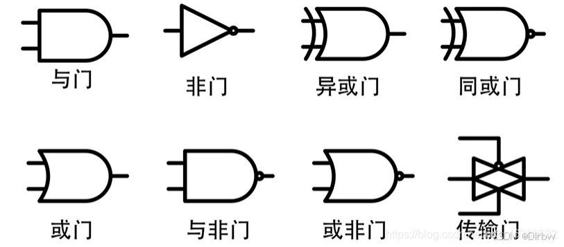
and:與門 ——a & b
or:非門——a | b
xor:異或門——a ^ b
nand:與非門——~(a & b)
nor:或非門——~(a | b)
xnor:同或門——~(a ^ b)
anotb:a and not b——a & ~b
解:
module top_module( input a, b,output out_and,output out_or,output out_xor,output out_nand,output out_nor,output out_xnor,output out_anotb
);assign out_and   =   a  &  b;assign out_or    =   a  |  b;assign out_xor   =   a  ^  b;assign out_nand  = ~(a  &  b);assign out_nor   = ~(a  |  b);assign out_xnor  = ~(a  ^  b);assign out_anotb =   a  &~ b;//a and not b:a與非b
endmodule
2. Truth tables
題目:
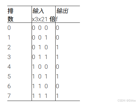
思路:從真值表綜合電路。
真值表共有8行,對應三個輸入的所有可能組合。輸出f為1的行是第2、3、5、7行。我需要把這些行的輸入條件找出來,然后轉換成邏輯表達式。
創建實現真值表函數的電路的一種簡單方法是以乘積總和的形式表示函數。乘積之和(即 OR )(即 AND)是指在真值表的每一行使用一個 N 輸入 AND 門(以檢測輸入何時與每一行匹配),后跟一個 OR 門,該門僅選擇導致“1”輸出的那些行。
行2:x3=0, x2=1, x1=0 → (~x3) & x2 & (~x1)
行3:x3=0, x2=1, x1=1 → (~x3) & x2 & x1
行5:x3=1, x2=0, x1=1 → x3 & (~x2) & x1
行7:x3=1, x2=1, x1=1 → x3 & x2 & x1
然后,這些四個與項需要或起來。所以最終的表達式應該是這四個項的或。
所以邏輯表達式為:
f = (~x3 & x2 & ~x1) | (~x3 & x2 & x1) | (x3 & ~x2 & x1) | (x3 & x2 & x1)
簡化后的表達式是:
f = (~x3 & x2) | (x3 & x1)
解:
module top_module( input x3,input x2,input x1,  // three inputsoutput f   // one output
);assign f = (~x3 & x2) | (x3 & x1);
endmodule
3. 256-to-1 4-bit multiplexer
題目:創建一個 4 位寬、256 對 1 的多路復用器。256 個 4 位輸入全部打包到一個 1024 位輸入向量中。sel=0 應該選擇 [3:0] 中的位,sel=1 選擇 [7:4] 中的位,sel=2 選擇 [11:8] 中的位,等等。
思路:確定sel的值映射到輸入向量的相應位置
解:
module top_module (input [1023:0] in,input [7:0] sel,output [3:0] out
);assign out = {in[sel*4+3], in[sel*4+2], in[sel*4+1], in[sel*4+0]}; //一一對應輸出// assign out = in[sel*4 +: 4];		// assign out = in[sel*4+3 -: 4];endmodule
4. 3-bit binary adder
題目:要求實現一個3-bit全加器
思路:有三種解決的方法。
1、反復使用的真值表轉為邏輯表達式
2、采用位拼接符號{ }進行對位的操作
3、例化1-bit全加器,使用三個1-bit全加器實現目標(這里采用)
解:
//方法3
module top_module( input [2:0] a, b,input cin,output [2:0] cout,output [2:0] sum
);adder u1 (.a(a[0]),.b(b[0]),.cin(cin),.cout(cout[0]),.sum(sum[0])
);adder u2 (.a(a[1]),.b(b[1]),.cin(cout[0]),.cout(cout[1]),.sum(sum[1])
);adder u3 (.a(a[2]),.b(b[2]),.cin(cout[1]),.cout(cout[2]),.sum(sum[2])
);
endmodule
module adder(//由于沒有例化好的adder模塊需要自己補上input a,b,cin,output cout,sum
);assign {cout,sum} = a + b + cin;
endmodule
5. Signed addition overflow
題目: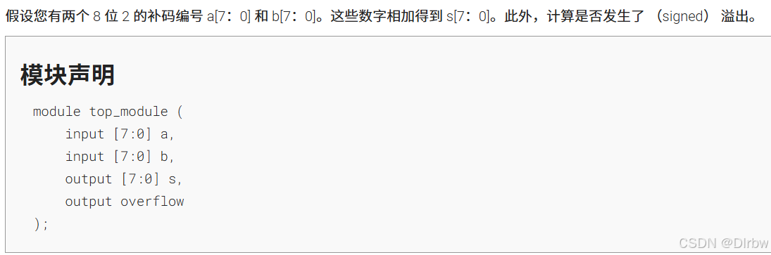
思路:要實現兩個8位補碼數的加法并檢測有符號溢出,需根據以下條件判斷溢出:
溢出 =(兩正數相加結果為負)或(兩負數相加結果為正)
加法可以直接用加法運算符實現,比如assign s = a + b;。
但是,溢出需要根據上述條件來判斷。例如,當a和b的最高位都為0(正數),而s的最高位為1(負數),則溢出;或者a和b的最高位都為1(負數),而s的最高位為0(正數),則溢出。
或者,另一種方法是檢查進位。補碼加法的溢出可以表示為:
溢出 = (a[7] & b[7] & ~s[7]) | (~a[7] & ~b[7] & s[7])。也就是說,當兩個操作數都是負數,但結果為正,或者兩個操作數都是正數,但結果為負時,溢出發生。
解:
module top_module (input [7:0] a,input [7:0] b,output [7:0] s,output overflow
); assign s = a + b;    // 直接計算和// 溢出條件:兩正數結果為負,或兩負數結果為正assign overflow = (a[7] & b[7] & ~s[7]) | (~a[7] & ~b[7] & s[7]);endmodule
6. 4-digit BCD adder
題目: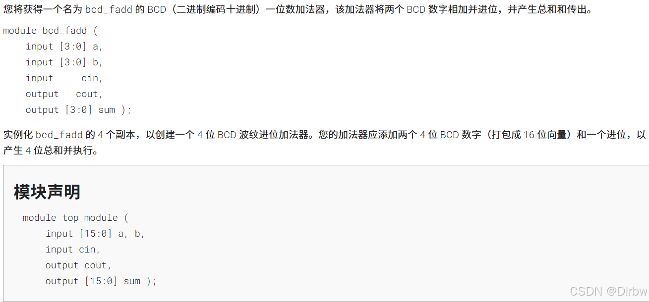
思路:例化bcd_fadd,使用四個bcd_fadd實現目標
解:
module top_module( input [15:0] a, b,input cin,output cout,output [15:0] sum );wire [3:0] cout_temp;bcd_fadd u1(.a(a[3:0]),.b(b[3:0]),.cin(cin),.cout(cout_temp[0]),.sum(sum[3:0]));bcd_fadd u2(.a(a[7:4]),.b(b[7:4]),.cin(cout_temp[0]),.cout(cout_temp[1]),.sum(sum[7:4]));bcd_fadd u3(.a(a[11:8]),.b(b[11:8]),.cin(cout_temp[1]),.cout(cout_temp[2]),.sum(sum[11:8]));bcd_fadd u4(.a(a[15:12]),.b(b[15:12]),.cin(cout_temp[2]),.cout(cout_temp[3]),.sum(sum[15:12]));assign cout = cout_temp[3];endmodule7. Minimum SOP and POS
題目: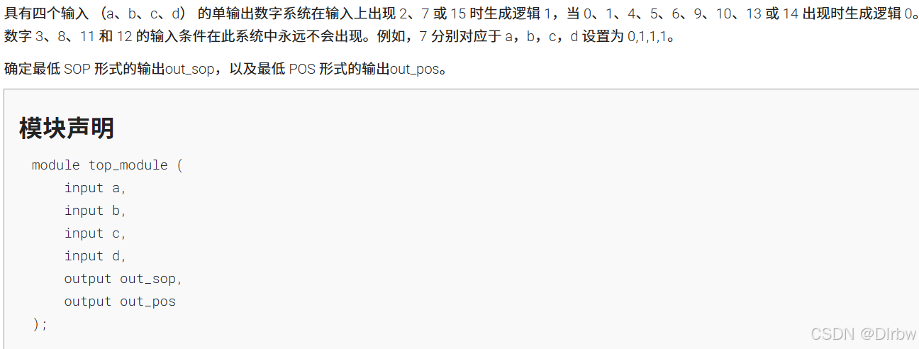
思路:按照題目要求畫出卡諾圖,注意abcd的權值順序:

畫出卡諾圖:
 對于SOP(積之和),即最小項之和。輸出為1的情況是2(0010)、7(0111)、15(1111)。所以需要將這些情況轉化為乘積項,然后合并。同時,無關項可以視情況加入,以簡化表達式。
同樣,POS(和之積)需要考慮輸出為0的情況,即當輸出為0時,對應的最大項需要被覆蓋。而無關項可能可以被用來簡化POS表達式。
解:
module top_module (input a,input b,input c,input d,output out_sop,output out_pos
); assign out_sop = (c & d)|(~a & ~b & c & ~d);assign out_pos = (c & ~b & ~a)|(c & d & ~a)|(c & d & b);
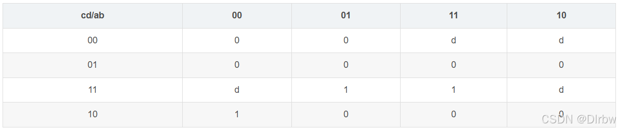
endmodule8. Karnaugh map
題目:
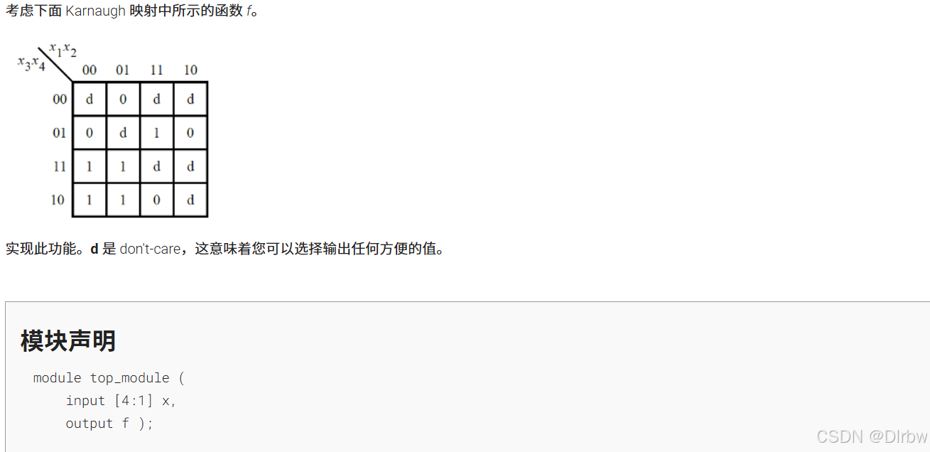
思路:通過ab來控制cd輸出的值,與上題的解決思路一樣。
解:
module top_module (input [4:1] x, output f );assign f = ( ~x[1] & x[3])|(x[1] & x[2] & ~x[3]);
endmodule
9. K-map implemented with a multiplexer
題目: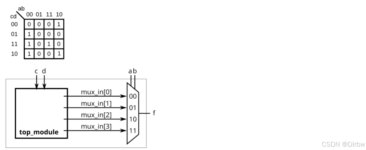
思路:
解:
module top_module (input c,input d,output [3:0] mux_in
); assign mux_in = {(c & d),(~d),(1'b0),(c|d)};
endmodule
總結
通過對組合邏輯類相關題目的練習,初步掌握了如何用verilog 語言來編寫邏輯門電路、多路復用器、還有真值表和卡諾圖能夠幫助我們解決問題,收獲頗多!
)

](http://pic.xiahunao.cn/算法刷題記錄——LeetCode篇(3.2) [第211~212題](持續更新))


>)


)


)


下RPCRT4!NMP_SyncSendRecv函數分析)