一、設計和優化3D光柵耦合器
1.1 代碼講解
通過預定義的環形間距參數(distances數組),在FDTD中生成橢圓光柵結構,并通過用戶交互確認幾何正確性后,可進一步執行參數掃描優化。
# os:用于操作系統相關功能(如文件路徑操作)
import os
import sys# lumapi:Lumerical 的 Python API,用于控制 FDTD 仿真
import lumapi
# math:數學計算(如三角函數)
import math
# numpy (np):數值計算(如數組操作)
import numpy as np
# scipy (sp) 和 scipy.interpolate:科學計算(如插值)
import scipy as sp
import scipy.interpolate# json:處理 JSON 文件
import json
# LumEncoder 和 LumDecoder:自定義 JSON 編碼/解碼器,用于處理 Lumerical 的特殊數據類型
from lumjson import LumEncoder, LumDecoder
# OrderedDict:保持鍵值對順序的字典
from collections import OrderedDict# 定這是一個光柵耦合器(Grating Coupler)的類,用于存儲和優化光柵耦合器的參數
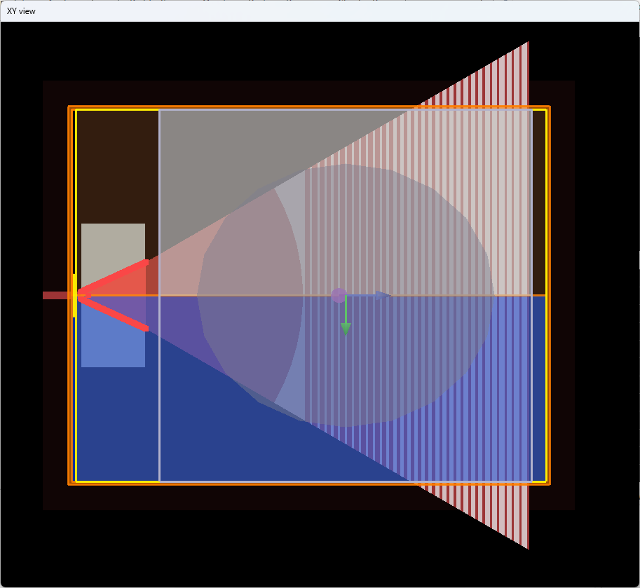
class GratingCoupler:"""Holds basic parameters of the grating coupler to optimize"""# __init__ 初始化方法 theta_fib_mat:光纖在材料中的入射角(單位:度,默認 8°) initial_theta_taper:初始錐角(單位:度,默認 30°) optim:是否啟用優化模式(默認 False)def __init__(self, lambda0, n_trenches, n_bg=1.44401, mat_bg="<Object defined dielectric>", n_wg=3.47668,mat_wg="<Object defined dielectric>", bandwidth=0, wg_height=220e-9, etch_depth=70e-9, wg_width=450e-9,theta_fib_mat=8, dx=30e-9, dzFactor=3, dim=2, polarization='TE', initial_theta_taper=30, optim=False):# 存儲輸入的中心波長、帶寬和光柵槽數self.lambda0 = lambda0self.bandwidth = bandwidth# n_trences:光柵槽的數量self.n_trenches = n_trenches# 存儲波導和背景的幾何與材料參數self.wg_height = wg_heightself.etch_depth = etch_depthself.wg_width = wg_width # < Only matters for 3D simulationself.material_name = mat_wgself.index_wg = n_wgself.n_bg = n_bg # background refractive indexself.mat_bg = mat_bg# 定義光纖的位置和模式尺寸self.x_fib = 18e-6 # 光纖位置(x 方向)self.x_fib_span = 26e-6 # < Roughly 2.5 * mode diameter 光纖模式直徑的 2.5 倍self.z_fib = 0.5e-6 # 光纖位置(z 方向)# 定義模式監視器的位置和尺寸(用于計算耦合效率)self.mode_pos_x = self.x_fib - self.x_fib_span / 2 - 1e-6 if dim == 2 else -1e-6self.mode_span_y = 3e-6 # 模式監視器的 y 方向跨度self.mode_span_z = 3e-6 # 模式監視器的 z 方向跨度# 定義光源的位置(稍微偏移以避免數值問題)self.bksrc_pos_x = self.mode_pos_x + 100e-9# 定義仿真網格的尺寸self.dzFactor = dzFactor # z 方向網格細化因子(默認 3)self.dx = dx # x 方向網格尺寸self.dy = dx # y 方向網格尺寸(與 dx 相同)self.dz = etch_depth / dzFactor # z 方向網格尺寸## Dimension of the simulation region# 定義仿真區域的邊界(x/y/z 方向的最小/最大值)self.x_min = self.mode_pos_x - 5 * self.dxself.x_max = self.x_fib + self.x_fib_span / 2 + 1e-6self.y_min = -self.x_fib_span / 2self.y_max = self.x_fib_span / 2self.z_min = -2.05e-6self.z_max = 1.5e-6# 定義優化區域的起始位置(僅優化光柵部分)self.x_min_opt_region = self.x_fib - self.x_fib_span / 2. if dim == 2 else self.mode_pos_x + 5 * dx# theta_fib_air = 10# theta_fib_mat = math.degrees(math.asin(math.sin(math.radians(theta_fib_air))/n_bg))# 計算光纖在空氣中的角度(基于 Snell 定律)self.theta_fib_mat = theta_fib_mat # math.degrees(math.asin(math.sin(math.radians(theta_fib_air))/n_bg))self.theta_fib_air = math.degrees(math.asin(math.sin(math.radians(self.theta_fib_mat)) * self.n_bg))# 填充因子(光柵槽寬度與周期的比例)self.F0 = 0.95 # < Starting value for the filling factor. Could be up to 1 but that would lead to very narrow trenches which can't be manufactured.# 定義連接波導和光柵的過渡區域(插值點用于平滑過渡)self.x_connector_start = -0.5e-6 # 連接器起始位置self.x_connector_end = 4.0e-6 # 連接器結束位置self.n_connector_pts = 28 # 連接器插值點數self.initial_points_x = np.linspace(self.x_connector_start, self.x_connector_end,self.n_connector_pts + 2) # < x-range for the connector region# 設置偏振模式和初始錐角self.pol_angle = 90 if polarization == 'TE' else 0 # TE: 90°, TM: 0°self.initial_theta_taper = initial_theta_taper # 初始錐角self.optim = optim # 是否啟用優化模式# 優化模式(optim=True):啟用高精度網格設置,用于最終參數優化,確保結果準確,但計算成本高。# 普通模式(optim=False):使用較粗網格,用于快速驗證或初步分析,節省計算資源。# 設置3D FDTD仿真項目的方法,包括仿真區域、光源、監視器等def setup_gratingcoupler_3d_base_project(self, fdtd):# """# Setup the basic 3D FDTD project with the simulation region, source, monitors, etc.# """## CLEAR SESSION# fdtd.clear()# 創建新的 FDTD 仿真項目fdtd.newproject()# fdtd = lumapi.FDTD(hide=False) # 創建FDTD實例,下載新版本還會出現之前的報錯的話把這行注釋掉## Start adding base components# 禁用圖形界面刷新,提升腳本執行速度 禁用圖形界面渲染功能,避免仿真過程中實時更新可視化結果,可降低系統資源消耗提升計算效率fdtd.redrawoff()## Set FDTD properties# anti-symmetric:適用于 TE 偏振的邊界條件(電場垂直于邊界)# conformal variant 0:標準共形網格細化方法(適合一般結構)props = OrderedDict([("dimension", "3D"),("x min", self.x_min),("x max", self.x_max),("y min", self.y_min),("y max", self.y_max),("z min", self.z_min),("z max", self.z_max),("background material", self.mat_bg),("y min bc", "anti-symmetric"), # y 下邊界條件(反對稱)("simulation time", 5000e-15),("auto shutoff min", 1e-6), # 自動停止閾值(場能量衰減到 1e-6 時停止)("mesh refinement", "conformal variant 0"), # 網格細化方法("meshing tolerance", 1.2e-15), # 網格容差(控制網格密度)控制網格生成精度閾值,數值越小網格越密集(1.2e-15為極高精度)("use legacy conformal interface detection", False) # 禁用舊版界面檢測,采用新版接口識別方法提升網格生成效率和準確性])# 處理背景材料和優化模式if self.mat_bg == "<Object defined dielectric>":props["index"] = self.n_bg # 自定義背景材料的折射率if self.optim:props["mesh refinement"] = "precise volume average" # 優化模式使用精確體積平均法props["meshing refinement"] = 11 # 網格細化級別(最高為 11)if self.pol_angle == 0:props["y min bc"] = "symmetric" # TM 偏振時使用對稱邊界條件# 根據屬性創建 FDTD 仿真區域fdtd.addfdtd(properties=props)# 添加高斯光源fdtd.addgaussian(name="source", injection_axis="z-axis", direction="backward",polarization_angle=self.pol_angle, # 偏振角度(TE:90°, TM:0°)x=self.x_fib, # 光源 x 位置(與光纖對齊)x_span=self.x_fib_span, # x 方向跨度(覆蓋光纖模式)y_min=self.y_min, y_max=self.y_max, z=self.z_fib, # z 位置(光纖高度)beam_parameters="Waist size and position", # 高斯光束參數模式waist_radius_w0=5.2e-6, # 束腰半徑 5.2 μmdistance_from_waist=0.0, # 束腰位置與光源重合angle_theta=self.theta_fib_mat, # 光在材料中的入射角度(例如 8°)center_wavelength=self.lambda0, wavelength_span=0.1e-6, # 波長范圍(100 nm)optimize_for_short_pulse=False) # 禁用短脈沖優化# 設置全局光源和監視器參數fdtd.setglobalsource("center wavelength", self.lambda0) # 全局光源中心波長fdtd.setglobalsource("wavelength span", 0.1e-6) # 全局波長范圍fdtd.setglobalsource("optimize for short pulse", False) # 禁用短脈沖優化fdtd.setglobalmonitor("frequency points", 11) # 監視器頻率點數,在波長范圍內均勻采樣 11 個點fdtd.setglobalmonitor("use wavelength spacing", True) # 使用波長間距(非頻率間距)# 添加光源區域網格 在光源區域設置更細的 z 方向網格,提高仿真精度(但默認不啟用)fdtd.addmesh(name="source_mesh", x=self.x_fib, x_span=24e-6, y_min=self.y_min, y_max=self.y_max, z=self.z_fib,z_span=2 * self.dz, override_x_mesh=False, override_y_mesh=False, override_z_mesh=True, dz=self.dz)fdtd.setnamed("source_mesh", "enabled", False) # < Disable by default but need to check the effect# 添加基底(Substrate)if self.material_name == "<Object defined dielectric>":fdtd.addrect(name="substrate", x_min=(self.x_min - 2e-6), x_max=(self.x_max + 2e-6), # 基底 x 范圍(超出仿真區域)y_min=(self.y_min - 2e-6), y_max=(self.y_max + 2e-6), z_min=-4e-6, z_max=-2e-6, # z 范圍(位于波導下方)material=self.material_name, index=self.index_wg, alpha=0.1) # 透明度(可視化用)else:# 預定義材料基底fdtd.addrect(name="substrate", x_min=(self.x_min - 2e-6), x_max=(self.x_max + 2e-6),y_min=(self.y_min - 2e-6), y_max=(self.y_max + 2e-6), z_min=-4e-6, z_max=-2e-6,material=self.material_name, alpha=0.1)# 添加模式監視器 FOM 監視器:測量光柵耦合器的耦合效率(傳輸到波導的光功率)fdtd.addpower(name="fom", monitor_type="2D X-normal", x=self.mode_pos_x, y=0, y_span=self.mode_span_y, z=0,z_span=self.mode_span_z)fdtd.addmesh(name="fom_mesh", x=self.mode_pos_x, x_span=2 * self.dx, y=0, y_span=self.mode_span_y, z=0,z_span=self.mode_span_z, override_x_mesh=True, dx=self.dx, override_y_mesh=False,override_z_mesh=False)# 添加優化區域監視器 記錄光柵區域的電場分布,用于后續優化算法分析fdtd.addpower(name="opt_fields", monitor_type="3D", x_min=self.x_min_opt_region, x_max=self.x_max,y_min=self.y_min, y_max=self.y_max, z_min=self.wg_height - self.etch_depth, z_max=self.wg_height,# z 最小值(刻蝕深度)z 最大值(波導高度)output_Hx=False, output_Hy=False, output_Hz=False, output_power=False) # 禁用磁場輸出 禁用功率輸出(僅保存電場)fdtd.addmesh(name="opt_fields_mesh", x_min=self.x_min_opt_region, x_max=self.x_max, y_min=self.y_min,y_max=self.y_max, z_min=self.wg_height - self.etch_depth, z_max=self.wg_height, dx=self.dx,dy=self.dy, dz=self.dz)# 添加折射率監視器fdtd.addindex(name="index_xy", monitor_type="2D Z-normal", x_min=self.x_min, x_max=self.x_max, y_min=self.y_min,y_max=self.y_max, z=self.wg_height - (self.etch_depth / 2.), # z 位置(刻蝕深度中點)spatial_interpolation='none', enabled=False) # 禁用空間插值 默認禁用fdtd.addindex(name="index_xz", monitor_type="2D Y-normal", x_min=self.x_min, x_max=self.x_max, y=0,z_min=self.z_min, z_max=self.z_max, spatial_interpolation='none', enabled=False)# 添加波導(Waveguide) 波導作用:連接光柵耦合器和芯片其他部分if self.material_name == "<Object defined dielectric>":fdtd.addrect(name='wg', x_min=(self.x_min - 2e-6), x_max=2e-6, y=0, y_span=self.wg_width, z_min=0,z_max=self.wg_height,material=self.material_name, index=self.index_wg)else:fdtd.addrect(name='wg', x_min=(self.x_min - 2e-6), x_max=2e-6, y=0, y_span=self.wg_width, z_min=0,z_max=self.wg_height, material=self.material_name)# 添加光柵環形結構 光柵結構:通過環形結構定義光柵的周期性刻蝕theta_start = self.initial_theta_tapertheta_stop = 360.0 - theta_start # 環形角度范圍(對稱)# if self.material_name == "<Object defined dielectric>":# fdtd.addring(name='silicon', x=0, y=0, z_min=0, z_max=self.wg_height, inner_radius=0, outer_radius=60e-6,# theta_start=theta_stop, theta_stop=theta_start, material=self.material_name,# index=self.index_wg)# else: # 預定義材料光柵# fdtd.addring(name='silicon', x=0, y=0, z_min=0, z_max=self.wg_height, inner_radius=0, outer_radius=60e-6,# theta_start=theta_stop, theta_stop=theta_start, material=self.material_name)if self.material_name == "<Object defined dielectric>":fdtd.addring(name='silicon', x=0, y=0, z_min=0, z_max=self.wg_height, inner_radius=0, outer_radius=60e-6, make_ellipsoid=True, outer_radius_2=60e-6, theta_start=theta_stop, theta_stop=theta_start, material=self.material_name, index=self.index_wg)else:fdtd.addring(name='silicon', x=0, y=0, z_min=0, z_max=self.wg_height, inner_radius=0, outer_radius=60e-6, make_ellipsoid=True, outer_radius_2=60e-6, theta_start=theta_stop, theta_stop=theta_start, material=self.mate


利用C11模擬偽閉包實現連接的安全回收)
:Agent系統的應用架構與落地實)


